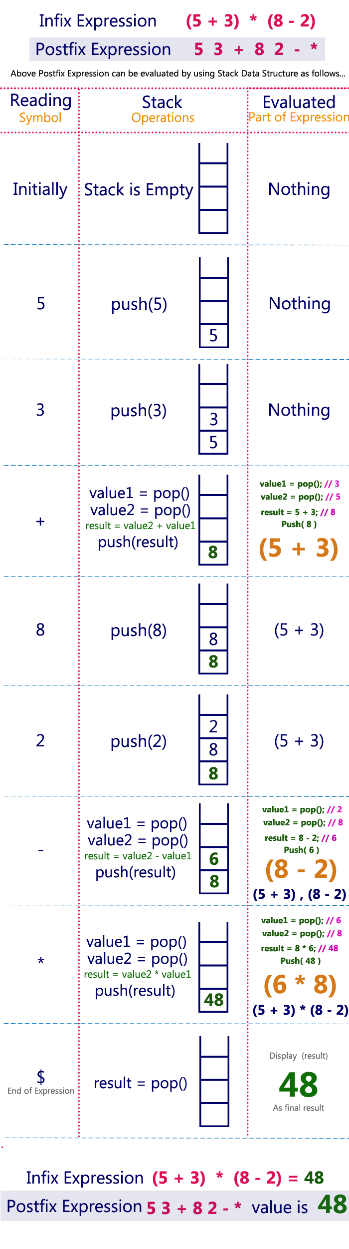
I highly recommend reading the Nand to Tetris book for anyone interested in learning how computers work from the ground up. This page is a result of my notes while reading the book. While most of the ideas come from the book, I have added some of my own thoughts and some external sources. I hope you find this page helpful.
🎯 Objective: Understand the basics of boolean logic and build all required logic gates from the NAND gate.
Modern computers store and process information stored as two-valued signals — called
A binary variable or a bit can represent two possible states: 0 and 1; off and on; false and true; no and yes; etc. binary variables can be used to represent states. e.g.
| 0 | 0 | 0 |
| 0 | 0 | 1 |
| 0 | 1 | 0 |
| 0 | 1 | 1 |
| 1 | 0 | 0 |
| 1 | 0 | 1 |
| 1 | 1 | 0 |
| 1 | 1 | 1 |
The total number of boolean functions for binary variables is , because:
0 or 1.e.g. There are distinct boolean functions for binary variables.
| Function | Expression | A=0, B=0 | A=0, B=1 | A=1, B=0 | A=1, B=1 |
|---|---|---|---|---|---|
| F0 | 0 | 0 | 0 | 0 | 0 |
| F1 | NOT A AND NOT B | 1 | 0 | 0 | 0 |
| F2 | NOT A AND B | 0 | 1 | 0 | 0 |
| F3 | NOT A | 1 | 1 | 0 | 0 |
| F4 | A AND NOT B | 0 | 0 | 1 | 0 |
| F5 | NOT B | 1 | 0 | 1 | 0 |
| F6 | XOR(A, B) | 0 | 1 | 1 | 0 |
| F7 | NAND(A, B) | 1 | 1 | 1 | 0 |
| F8 | A AND B | 0 | 0 | 0 | 1 |
| F9 | XNOR(A, B) | 1 | 0 | 0 | 1 |
| F10 | B | 0 | 1 | 0 | 1 |
| F11 | NOT A OR B | 1 | 1 | 0 | 1 |
| F12 | A | 0 | 0 | 1 | 1 |
| F13 | A OR NOT B | 1 | 0 | 1 | 1 |
| F14 | A OR B | 0 | 1 | 1 | 1 |
| F15 | 1 | 1 | 1 | 1 | 1 |
A
Since all logic gates have the same input and output data type (i.e. binary), they can be combined, creating composite gates of arbitrary complexity. e.g. Xor = Or(And(a, Not(b)), And(Not(a), b)).
Any given logic gate can be viewed from two perspective:
A
The designer specifies the chip logic by writing a HDL program, which is then subjected to a rigorous battery of tests. The tests are carried out virtually, using computer simulation: A special software tool, called a hardware simulator, takes the HDL program as input and creates a software representation of the chip logic. Next, the designer can instruct the simulator to test the virtual chip on various sets of inputs. The simulator computes the chip outputs, which are then compared to the desired outputs.
The hardware simulator can also simulate and quantify the performance characteristics (energy consumption, computational speed, cost) of a chip.
The specifications of the logic gates needed to build the chips of our computer system are given below.
First, the primitive Not(And(a, b)).
Truth table:
| a | b | Nand(a, b) |
|---|---|---|
| 0 | 0 | 1 |
| 0 | 1 | 1 |
| 1 | 0 | 1 |
| 1 | 1 | 0 |
API:
| Chip name | Nand |
| Input | a, b |
| Output | out |
| Function | if ((a == 1) and (b==1)) then out = 0, else out = 1 |
The NAND gate is called a primitive gate because it can be used to implement any boolean function. Proof:
Various subsets of logical operators can be used for expressing any boolean function, and { And, Or, Not } is one such subset. NAND can be used to implement each member of the subset as demonstrated below.
NOT(a) = NAND(a, a)
AND(a, b) = NOT(NAND(a, b))
OR(a, b) = NOT(NOT(a) AND NOT(b)) (De morgan law); This is equivalent to: OR(a, b) = NAND(NOT(a), NOT(b))
Next, we look at a set of four gates that implement

Truth table:
| a | Not(a) |
|---|---|
| 0 | 1 |
| 1 | 0 |
API:
| Chip name | Not |
| Input | in |
| Output | out |
| Function | if (in == 0) then out = 1, else out = 0 |
HDL:
CHIP Not {

IN in;

OUT out;


PARTS:

Nand(a= in, b= in, out= out);

}
The next classical gate is the

Truth table:
| a | b | And(a, b) |
|---|---|---|
| 0 | 0 | 0 |
| 0 | 1 | 0 |
| 1 | 0 | 0 |
| 1 | 1 | 1 |
API:
| Chip name | And |
| Input | a, b |
| Output | out |
| Function | if ((a == 1) and (b==1)) then out = 1, else out = 0 |
HDL:
CHIP And {

IN a, b;

OUT out;

PARTS:

Nand(a= a, b= b, out= nandout);

Not(in= nandout, out= out);

}
The

Truth table:
| a | b | Or(a, b) |
|---|---|---|
| 0 | 0 | 0 |
| 0 | 1 | 1 |
| 1 | 0 | 1 |
| 1 | 1 | 1 |
API:
| Chip name | Or |
| Input | a, b |
| Output | out |
| Function | if ((a == 0) and (b == 0)) then out = 0, else out = 1 |
HDL:
CHIP Or {

IN a, b;

OUT out;


PARTS:

Not(in= a, out= nota);

Not(in= b, out= notb);

And(a= nota, b= notb, out= notaandnotb);

Not(in= notaandnotb, out= out);

}
The last classical gate we will build is the

Truth table:
| a | b | Xor(a, b) |
|---|---|---|
| 0 | 0 | 0 |
| 0 | 1 | 1 |
| 1 | 0 | 1 |
| 1 | 1 | 0 |
API:
| Chip name | Xor |
| Input | a, b |
| Output | out |
| Function | if (a != b) then out = 1, else out = 0 |
HDL:
CHIP Xor {

IN a, b;

OUT out;


PARTS:

Not(in= a, out= nota);

Not(in= b, out= notb);

And(a= a, b= notb, out= aandnotb);

And(a= b, b= nota, out= bandnota);

Or(a= aandnotb, b= bandnota, out= out);

}
Next, we look at a set of a and b, are interpreted as data bits, and a third bit, named sel, is interpreted as a sel to select and output the value of either a or b.
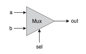
Truth table:
| a | b | sel | out |
|---|---|---|---|
| 0 | 0 | 0 | 0 |
| 0 | 0 | 1 | 0 |
| 0 | 1 | 0 | 0 |
| 0 | 1 | 1 | 1 |
| 1 | 0 | 0 | 1 |
| 1 | 0 | 1 | 0 |
| 1 | 1 | 0 | 1 |
| 1 | 1 | 1 | 1 |
API:
| Chip name | Mux |
| Input | a, b, sel |
| Output | out |
| Function | if (sel == 0) then out = a, else out = b |
HDL:
CHIP Mux {

IN a, b, sel;

OUT out;


PARTS:

Not(in= sel, out= notsel);

And(a= a, b= notsel, out= aandnotsel);

And(a= b, b= sel, out= bandsel);

Or(a= aandnotsel, b= bandsel, out= out);

}
Next is the
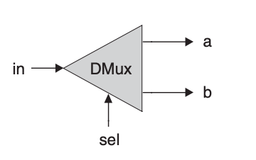
| in | sel | a | b |
|---|---|---|---|
| 0 | 0 | 0 | 0 |
| 0 | 1 | 0 | 0 |
| 1 | 0 | 1 | 0 |
| 1 | 1 | 0 | 1 |
API:
| Chip name | DMux |
| Input | in, sel |
| Output | a, b |
| Function | if (sel == 0) then {a, b} = {in, 0}, else {a, b} = {0, in} |
HDL:
CHIP DMux {

IN in, sel;

OUT a, b;


PARTS:

Not(in= sel, out= notsel);

And(a= in, b= notsel, out= a);

And(a= in, b= sel, out= b);

}
Now, we explore in and out represent 16-bit values, then out [3] = in[5] sets the 3rd bit of out to the value of the 5th bit of in. The bits are indexed from right to left, the rightmost bit being the 0’th bit and the leftmost bit being the 15’th bit (in a 16-bit setting).
The first multi-bit gate we will build is the Not to every one of the input bits.
API:
| Chip name | Not16 |
| Input | in[16] |
| Output | out[16] |
| Function | for i = 0..15 out[i] = Not(in[i]) |
HDL:
CHIP Not16 {

IN in[16];

OUT out[16];


PARTS:

Not(in= in[0], out= out[0]);

Not(in= in[1], out= out[1]);

Not(in= in[2], out= out[2]);

Not(in= in[3], out= out[3]);

Not(in= in[4], out= out[4]);

Not(in= in[5], out= out[5]);

Not(in= in[6], out= out[6]);

Not(in= in[7], out= out[7]);

Not(in= in[8], out= out[8]);

Not(in= in[9], out= out[9]);

Not(in= in[10], out= out[10]);

Not(in= in[11], out= out[11]);

Not(in= in[12], out= out[12]);

Not(in= in[13], out= out[13]);

Not(in= in[14], out= out[14]);

Not(in= in[15], out= out[15]);

}
Next is the And to every one of the input bits.
API:
| Chip name | And16 |
| Input | a[16], b[16] |
| Output | out[16] |
| Function | for i = 0..15 out[i] = And(a[i], b[i]) |
HDL:
CHIP And16 {

IN a[16], b[16];

OUT out[16];


PARTS:

And(a= a[0], b= b[0], out= out[0]);

And(a= a[1], b= b[1], out= out[1]);

And(a= a[2], b= b[2], out= out[2]);

And(a= a[3], b= b[3], out= out[3]);

And(a= a[4], b= b[4], out= out[4]);

And(a= a[5], b= b[5], out= out[5]);

And(a= a[6], b= b[6], out= out[6]);

And(a= a[7], b= b[7], out= out[7]);

And(a= a[8], b= b[8], out= out[8]);

And(a= a[9], b= b[9], out= out[9]);

And(a= a[10], b= b[10], out= out[10]);

And(a= a[11], b= b[11], out= out[11]);

And(a= a[12], b= b[12], out= out[12]);

And(a= a[13], b= b[13], out= out[13]);

And(a= a[14], b= b[14], out= out[14]);

And(a= a[15], b= b[15], out= out[15]);

}
Followed by the Or to every one of the input bits.
API:
| Chip name | Or16 |
| Input | a[16], b[16] |
| Output | out[16] |
| Function | for i = 0..15 out[i] = Or(a[i], b[i]) |
HDL:
CHIP Or16 {

IN a[16], b[16];

OUT out[16];


PARTS:

Or(a= a[0], b= b[0], out= out[0]);

Or(a= a[1], b= b[1], out= out[1]);

Or(a= a[2], b= b[2], out= out[2]);

Or(a= a[3], b= b[3], out= out[3]);

Or(a= a[4], b= b[4], out= out[4]);

Or(a= a[5], b= b[5], out= out[5]);

Or(a= a[6], b= b[6], out= out[6]);

Or(a= a[7], b= b[7], out= out[7]);

Or(a= a[8], b= b[8], out= out[8]);

Or(a= a[9], b= b[9], out= out[9]);

Or(a= a[10], b= b[10], out= out[10]);

Or(a= a[11], b= b[11], out= out[11]);

Or(a= a[12], b= b[12], out= out[12]);

Or(a= a[13], b= b[13], out= out[13]);

Or(a= a[14], b= b[14], out= out[14]);

Or(a= a[15], b= b[15], out= out[15]);

}
Finally, the
API:
| Chip name | Mux16 |
| Input | a[16], b[16], sel |
| Output | out[16] |
| Function | if (sel == 0) then for i = 0..15 out[i] = a[i], else for i = 0..15 out[i] = b[i] |
HDL:
CHIP Mux16 {

IN a[16], b[16], sel;

OUT out[16];


PARTS:

Mux(a= a[0], b= b[0], sel= sel, out= out[0]);

Mux(a= a[1], b= b[1], sel= sel, out= out[1]);

Mux(a= a[2], b= b[2], sel= sel, out= out[2]);

Mux(a= a[3], b= b[3], sel= sel, out= out[3]);

Mux(a= a[4], b= b[4], sel= sel, out= out[4]);

Mux(a= a[5], b= b[5], sel= sel, out= out[5]);

Mux(a= a[6], b= b[6], sel= sel, out= out[6]);

Mux(a= a[7], b= b[7], sel= sel, out= out[7]);

Mux(a= a[8], b= b[8], sel= sel, out= out[8]);

Mux(a= a[9], b= b[9], sel= sel, out= out[9]);

Mux(a= a[10], b= b[10], sel= sel, out= out[10]);

Mux(a= a[11], b= b[11], sel= sel, out= out[11]);

Mux(a= a[12], b= b[12], sel= sel, out= out[12]);

Mux(a= a[13], b= b[13], sel= sel, out= out[13]);

Mux(a= a[14], b= b[14], sel= sel, out= out[14]);

Mux(a= a[15], b= b[15], sel= sel, out= out[15]);

}
The last set of gates we will build are the
The first gate in this set is the Or gate outputs 1 when at least one of its m input bits is 1, and 0 otherwise. Our target computer will need an 8-way variant of this gate:
| Chip name | Or8Way |
| Input | in[8] |
| Output | out |
| Function | out = Or(in[0], in[1], ..., in[7]) |
CHIP Or8Way {

IN in[8];

OUT out;


PARTS:

Or(a= in[0], b= in[1], out= in01);

Or(a= in01, b= in[2], out= in012);

Or(a= in012, b= in[3], out= in0123);

Or(a= in0123, b= in[4], out= in01234);

Or(a= in01234, b= in[5], out= in012345);

Or(a= in012345, b= in[6], out= in0123456);

Or(a= in0123456, b= in[7], out= out);

}
Next, we build a
Our target computer platform requires two variants of this chip: a 4-way 16-bit multiplexer and an 8-way 16-bit multiplexer.
API:
| Chip name | Mux4Way16 |
| Input | a[16], b[16], c[16], d[16], sel[2] |
| Output | out[16] |
| Function | if (sel == 00) then out = a,else if (sel == 01) then out = b,else if (sel == 10) then out = c,else if (sel == 11) then out = d |
| Chip name | Mux8Way16 |
| Input | a[16], b[16], c[16], d[16], e[16], f[16], g[16], h[16], sel[3] |
| Output | out[16] |
| Function | if (sel == 000) then out = a,else if (sel == 001) then out = b,else if (sel == 010) then out = c,else if (sel == 011) then out = delse if (sel == 100) then out = e,else if (sel == 101) then out = f,else if (sel == 110) then out = g,else if (sel == 111) then out = h |
HDL:
CHIP Mux4Way16 {

IN a[16], b[16], c[16], d[16], sel[2];

OUT out[16];

// If you look at the truth table, you can see that the sel[0] bit selects between a/b (first group) and c/d (second group),
and the sel[1] bit selects between the outputs of the first group and the second group.
PARTS:

// First level: Select between a/b and c/d using sel[0]

Mux16(a=a, b=b, sel=sel[0], out=ab); // ab is the output of first Mux16

Mux16(a=c, b=d, sel=sel[0], out=cd); // cd is the output of second Mux16


// Second level: Select between ab and cd using sel[1]

Mux16(a=ab, b=cd, sel=sel[1], out=out);

}
CHIP Mux8Way16 {

IN a[16], b[16], c[16], d[16],

e[16], f[16], g[16], h[16],

sel[3];

OUT out[16];


PARTS:

Mux4Way16(a= a, b= b, c= c, d= d, sel= sel[0..1], out= abcd);

Mux4Way16(a= e, b= f, c= g, d= h, sel= sel[0..1], out= efgh);

Mux16(a= abcd, b= efgh, sel= sel[2], out= out);

}
Finally, we build a 0. The selection is specified by a set of selection bits, where .
Our target computer platform requires two variants of this chip: a 4-way 1-bit demultiplexer and an 8-way 1-bit demultiplexer.
API:
| Chip name | DMux4Way |
| Input | in, sel[2] |
| Output | a, b, c, d |
| Function | if (sel == 00) then {a, b, c, d} = {in, 0, 0, 0},else if (sel == 01) then {a, b, c, d} = {0, in, 0, 0},else if (sel == 10) then {a, b, c, d} = {0, 0, in, 0},else if (sel == 11) then {a, b, c, d} = {0, 0, 0, in} |
HDL:
CHIP DMux4Way {

IN in, sel[2];

OUT a, b, c, d;

// Performs the inverse of the multi-way multiplexer operation.
PARTS:

DMux(in= in, sel= sel[1], a= first, b= second);

DMux(in= first, sel= sel[0], a= a, b= b);

DMux(in= second, sel= sel[0], a= c, b= d);

}
| Chip name | DMux8Way |
| Input | in, sel[3] |
| Output | a, b, c, d, e, f, g, h |
| Function | if (sel == 000) then {a, b, c, …, h} = {1, 0, 0, 0, 0, 0, 0, 0},else if (sel == 001) then {a, b, c, …, h} = {0, 1, 0, 0, 0, 0, 0, 0},if (sel == 010) then {a, b, c, …, h} = {0, 0, 1, 0, 0, 0, 0, 0},… if (sel == 111) then {a, b, c, …, h} = {0, 0, 0, 0, 0, 0, 0, 1} |
HDL:
CHIP DMux8Way {

IN in, sel[3];

OUT a, b, c, d, e, f, g, h;


PARTS:

DMux(in= in, sel= sel[2], a= first, b= second);

DMux4Way(in= first, sel= sel[0..1], a= a, b= b, c= c, d= d);

DMux4Way(in= second, sel= sel[0..1], a= e, b= f, c= g, d= h);

}
🎯 Objective: Use the gates from chapter 1 to build an ALU (Arithmetic logic unit).
The
A
e.g.
=
=
=
A
In a
Computers represent numbers in binary. Any number can be represented by a sequence of bits (binary digits), which in turn may be represented by any mechanism capable of being in two mutually exclusive states.
Integer numbers are
The three common methods of extending the binary numeral system to represent
Of the three, two’s complement is the most commonly used today.
A
The two's complement of an N-bit number is the complement of that number with respect to (this is the property that gives this system its name). i.e. Given that is an N-bit number and is its two's complement, then . e.g.
If,
Then, (x's two's complement) because:
| Bits | Signed value (Two's complement) | Unsigned value |
|---|---|---|
| 000 | 0 | 0 |
| 001 | 1 | 1 |
| 010 | 2 | 2 |
| 011 | 3 | 3 |
| 100 | -4 | 4 |
| 101 | -3 | 5 |
| 110 | -2 | 6 |
| 111 | -1 | 7 |
Here is
Given , these are some examples:
| Addition in the two's complement system | Addition modulo |
|---|---|
| (represented as in binary) | (the two's complement representation of ) |
| (represented as in binary) | (the two's complement representation of ) |
| (represented as in binary) | (the two's complement representation of ) |
The
The material implications of these theoretical results are significant:
A
1 1 1 1 1 (carried bits )

  0 1 1 0 1 (13_10)

+ 1 0 1 1 1 (23_10)

-------------

1 0 0 1 0 0 (36_10)
When adding in the two's complement system, any extra carry bit is discarded, such that the result and the addends always have the same number of bits. This is effectively the same as applying the
An
A
| Chip name | HalfAdder |
| Input | a, b |
| Output | sum, carry |
| Function | sum = LSB of a + bcarry = MSB of a + b |
An inspection of the truth table reveals that the outputs sum(a, b) and carry(a, b) are identical to those of two simple Boolean functions Xor and And respectively.
| a | b | carry | sum |
|---|---|---|---|
| 0 | 0 | 0 | 0 |
| 0 | 1 | 0 | 1 |
| 1 | 0 | 0 | 1 |
| 1 | 1 | 1 | 0 |
/**
* Computes the sum of two bits.
*/
CHIP HalfAdder {

IN a, b; // 1-bit inputs

OUT sum, // Right bit of a + b

carry; // Left bit of a + b

PARTS:

And(a= a, b= b, out= carry);

Xor(a = a, b = b, out = sum);
}
A
| Chip name | FullAdder` |
| Input | a, b, c |
| Output | sum, carry |
| Function | sum = LSB of a + b + ccarry = MSB of a + b + c |
| a | b | c | carry | sum |
|---|---|---|---|---|
| 0 | 0 | 0 | 0 | 0 |
| 0 | 0 | 1 | 0 | 1 |
| 0 | 1 | 0 | 0 | 1 |
| 0 | 1 | 1 | 1 | 0 |
| 1 | 0 | 0 | 0 | 1 |
| 1 | 0 | 1 | 1 | 0 |
| 1 | 1 | 0 | 1 | 0 |
| 1 | 1 | 1 | 1 | 1 |
The names Half-adder and Full-adder derive from the implementation detail that a full-adder chip can be realized from two half-adders (and one other basic chip).
/**
* Computes the sum of three bits.
*/

CHIP FullAdder {

IN a, b, c; // 1-bit inputs

OUT sum, // Right bit of a + b + c

carry; // Left bit of a + b + c

PARTS:

HalfAdder(a= a, b= b, sum= partialSum, carry= partialCarry);

HalfAdder(a= partialSum, b= c, sum= sum, carry= partialCarry2);

Or(a= partialCarry, b= partialCarry2, out= carry);
}
An
| Chip name | Add16 |
| Input | a[16], b[16] |
| Output | out[16] |
| Function | Adds two 16-bit numbers. |
| Comment | The overflow bit is ignored. |
The addition of two n-bit numbers can be done bitwise, from right to left (from LSB pairs to MSB pairs). In each step, the resulting carry bit from the previous step is fed into the addition.
/**
* 16-bit adder: Adds two 16-bit two's complement values.
* The most significant carry bit is ignored.
*/

CHIP Add16 {

IN a[16], b[16];

OUT out[16];


PARTS:

FullAdder(a= a[0], b= b[0], c= false, sum= out[0], carry= carry0);

FullAdder(a= a[1], b= b[1], c= carry0, sum= out[1], carry= carry1);

FullAdder(a= a[2], b= b[2], c= carry1, sum= out[2], carry= carry2);

FullAdder(a= a[3], b= b[3], c= carry2, sum= out[3], carry= carry3);

FullAdder(a= a[4], b= b[4], c= carry3, sum= out[4], carry= carry4);

FullAdder(a= a[5], b= b[5], c= carry4, sum= out[5], carry= carry5);

FullAdder(a= a[6], b= b[6], c= carry5, sum= out[6], carry= carry6);

FullAdder(a= a[7], b= b[7], c= carry6, sum= out[7], carry= carry7);

FullAdder(a= a[8], b= b[8], c= carry7, sum= out[8], carry= carry8);

FullAdder(a= a[9], b= b[9], c= carry8, sum= out[9], carry= carry9);

FullAdder(a= a[10], b= b[10], c= carry9, sum= out[10], carry= carry10);

FullAdder(a= a[11], b= b[11], c= carry10, sum= out[11], carry= carry11);

FullAdder(a= a[12], b= b[12], c= carry11, sum= out[12], carry= carry12);

FullAdder(a= a[13], b= b[13], c= carry12, sum= out[13], carry= carry13);

FullAdder(a= a[14], b= b[14], c= carry13, sum= out[14], carry= carry14);

FullAdder(a= a[15], b= b[15], c= carry14, sum= out[15], carry= carry15);
}
An 1 to a given number. Although, the x + 1 operation can be realized with the general-purpose Adder chip, a dedicated Incrementer chip can do it more efficiently.
| Chip name | Inc16 |
| Input | in[16] |
| Output | out[16] |
| Function | out = in + 1 |
| Comment | The overflow bit is ignored. |
/**
* 16-bit incrementer:
* out = in + 1
*/

CHIP Inc16 {

IN in[16];

OUT out[16];

PARTS:

Add16(a = in, b[0] = true, b[1..15] = false, out = out);

}
The
| x | y | zx | nx | zy | ny | f | no | out | Description |
|---|---|---|---|---|---|---|---|---|---|
| 0 | y | 1 | 0 | 1 | 0 | 1 | 0 | 0 | 0 (constant zero) |
| 1 | y | 1 | 1 | 1 | 1 | 1 | 1 | 1 | 1 (constant one) |
| -1 | y | 1 | 1 | 1 | 0 | 1 | 0 | -1 | -1 (constant minus one) |
| x | y | 0 | 0 | 1 | 1 | 0 | 0 | x | x |
| x | y | 1 | 1 | 0 | 0 | 0 | 0 | y | y |
| x | y | 0 | 0 | 1 | 1 | 0 | 1 | ¬x | NOT x |
| x | y | 1 | 1 | 0 | 0 | 0 | 1 | ¬y | NOT y |
| x | y | 0 | 0 | 1 | 1 | 1 | 1 | -x | -x |
| x | y | 1 | 1 | 0 | 0 | 1 | 1 | -y | -y |
| x | y | 0 | 1 | 1 | 1 | 1 | 1 | x+1 | x + 1 |
| x | y | 1 | 1 | 0 | 1 | 1 | 1 | y+1 | y + 1 |
| x | y | 0 | 0 | 1 | 1 | 1 | 0 | x-1 | x - 1 |
| x | y | 1 | 1 | 0 | 0 | 1 | 0 | y-1 | y - 1 |
| x | y | 0 | 0 | 0 | 0 | 1 | 0 | x+y | x + y |
| x | y | 0 | 1 | 0 | 0 | 1 | 1 | x-y | x - y |
| x | y | 0 | 0 | 0 | 1 | 1 | 1 | y-x | y - x |
| x | y | 0 | 0 | 0 | 0 | 0 | 0 | x&y | x AND y |
| x | y | 0 | 1 | 0 | 1 | 0 | 1 | x|y | x OR y |
The Hack ALU operates on two 16-bit two's complement integers denoted x and y, and on six 1-bit inputs, called
1. if (zx) then x = 0 else x = x

2. if (nx) then x = !x else x = x

3. if (zy) then y = 0 else y = y

4. if (ny) then y = !y else y = y

5. if (f) then out = x + y else out = x and y

6. if (no) then out = !out else out = out
It may be instructive to describe the thought process that led to the design of this particular ALU. First, we made a list of all the primitive operations that we wanted our computer to be able to perform. Next, we used backward reasoning to figure out how
x,y, andoutcan be manipulated in binary fashion in order to carry out the desired operations. These processing requirements, along with our objective to keep the ALU logic as simple as possible, have led to the design decision to use six control bits, each associated with a straightforward binary operation.
/**

* ALU (Arithmetic Logic Unit):

* Computes out = one of the following functions:

* 0, 1, -1,

* x, y, !x, !y, -x, -y,

* x + 1, y + 1, x - 1, y - 1,

* x + y, x - y, y - x,

* x & y, x | y

* on the 16-bit inputs x, y,

* according to the input bits zx, nx, zy, ny, f, no.

* In addition, computes the two output bits:

* if (out == 0) zr = 1, else zr = 0

* if (out < 0) ng = 1, else ng = 0

*/

// Implementation: Manipulates the x and y inputs

// and operates on the resulting values, as follows:

// if (zx == 1) sets x = 0 // 16-bit constant

// if (nx == 1) sets x = !x // bitwise not

// if (zy == 1) sets y = 0 // 16-bit constant

// if (ny == 1) sets y = !y // bitwise not

// if (f == 1) sets out = x + y // integer 2's complement addition

// if (f == 0) sets out = x & y // bitwise and

// if (no == 1) sets out = !out // bitwise not


CHIP ALU {

IN

x[16], y[16], // 16-bit inputs

zx, // zero the x input?

nx, // NOT the x input?

zy, // zero the y input?

ny, // NOT the y input?

f, // compute (out = x + y) or (out = x & y)?

no; // NOT the out output?

OUT

out[16], // 16-bit output

zr, // if (out == 0) equals 1, else 0

ng; // if (out < 0) equals 1, else 0


PARTS:

// x's pre-processing

Mux16(a= x, sel= zx, out= x1);

Not16(in= x1, out= x1Notted);

Mux16(a= x1, b= x1Notted, sel= nx, out= x2);


// y's pre-processing

Mux16(a= y, sel= zy, out= y1);

Not16(in= y1, out= y1Notted);

Mux16(a= y1, b= y1Notted, sel= ny, out= y2);


// function

Add16(a = x2, b = y2, out = summed);

And16(a = x2, b = y2, out = andded);

Mux16(a= andded, b= summed, sel= f, out= out1);


// output post-processing

Not16(in= out1, out= out1Notted);

Mux16(a= out1, b= out1Notted, sel= no, out= out, out[15]= outFirst, out[0..7]= outLeft, out[8..15]= outRight);


// ng status bit

And(a= true, b= outFirst, out=ng);


// zr status bit

Or8Way(in= outLeft, out= isOutLeftAllZeroes);

Or8Way(in= outRight, out= isOutRightAllZeroes);

Or(a= isOutLeftAllZeroes, b= isOutRightAllZeroes, out= isOutLeftOrRightAllZeroes);

Not(in= isOutLeftOrRightAllZeroes, out= zr);

}
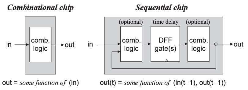
There are two types of chips:
A
A flip-flop encapsulates the intricate art of synchronization, clocking, and feedback loops that are essential for building sequential chips.
Using these flip-flops as elementary building blocks, we will specify and build all the memory devices employed by a typical modern computer: registers, RAMs, and counters.
This effort will complete the construction of the chip set needed to build an entire computer.
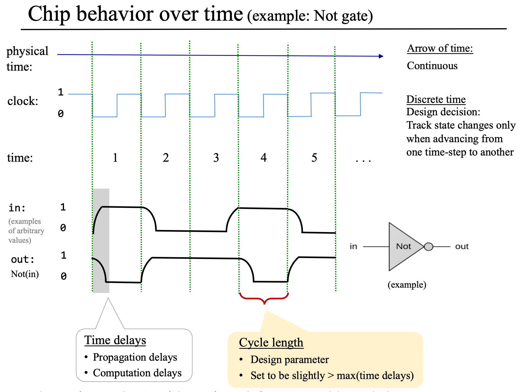
The act of "remembering something" is inherently time-dependent: You remember now what has been committed to memory before. Thus, in order to build chips that "remember" information, we must first develop some standard means for representing the progression of time.
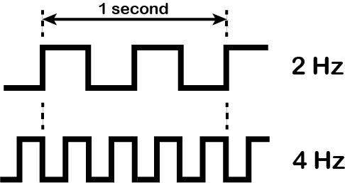
In most computers, the progression of time is regulated by a 0 (called low/tick) and 1 (called high/tock), at a regular pace.
The clock hardware implementation is usually an oscillator that generates a square wave. The frequency of the clock signal is measured in Hertz (Hz), which is the number of oscillations per second.
The elapsed time between the beginning of a "tick" and the end of a subsequent "tock" is called a
The clock is used to synchronize the sequential chips. Using the hardware’s circuitry, this signal is simultaneously broadcast to every sequential chip throughout the computer platform.
There are several variants of a flip-flop. We use a variant called the
A DFF is a simple memory element that stores a single bit. It has a data input in, a clock input load, and an output out. When the clock input is 1, the flip-flop copies the value of the data input to its output. When the clock input is 0, the flip-flop holds its previous value.
Taken together, both inputs enables the DFF to implement the behavior out(t) = in(t-1), where t is the current clock cycle. In other words, the DFF outputs the input value from the previous clock cycle.
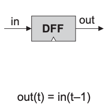
| Chip name | DFF |
| Input | in, load |
| Output | out |
| Function | out(t) = in(t-1) |
| Comment | This clocked gate has a built-in implementation and thus there is no need to implement it. |
[...] When the clock input is
1, the flip-flop copies the value of the data input to its output. When the clock input is0, the flip-flop holds its previous value.
Actually, what we described previously is a latch: which is level-triggered.
A DFF is edge-triggered. Our DFF will be rising edge-triggered, meaning it only copies the in data input when the clock signal transitions from 0 to 1.
All DFFs in a computer are connected to the same clock signal.
This reliable and predictable behavior of DFFs is crucial for data synchronization across the computer platform. There are physical delays in the propagation of signals through the computer’s hardware, e.g. It takes some time for the input into the ALU to stabilize and for the ALU to compute its output.
We solve this problem by using
A out = out(t-1).
A DFF, on the other hand, can only output its previous input, namely, out = in(t-1). We can build a register from a DFF, however, we must consider the following:
A natural way to build our register is to use a multiplexor: the "select bit" of the multiplexor becomes the "load bit" of the overall register chip:
If we want the register to start storing a new value, we can put this value in the
ininput and set the load bit to1; if we want the register to keep storing its internal value until further notice, we can set the load bit to0.
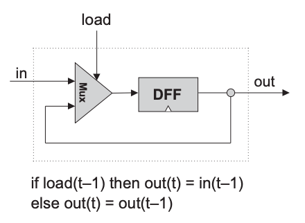
| Chip name | Bit or Binary cell (Single bit register) |
| Input | in, load |
| Output | out |
| Function | if (load(t-1) == 1) out(t) = in(t-1) else out(t) = out(t-1) |
CHIP Bit {
    IN in, load;
    OUT out;

    PARTS:
    DFF(in= dffIn, out= dffOut, out= out);
    Mux(a= dffOut, b= in, sel= load, out= dffIn);
}
A multi-bit register of w can be constructed from an array of w 1-bit registers. The basic design parameter of such a register is its width — the number of bits that it holds — e.g., 16, 32, or 64.
The multi-bit contents of such registers are typically referred to as words.
| Chip name | Register |
| Input | in[16], load |
| Output | out[16] |
| Function | if (load(t-1) == 1) out(t) = in(t-1) else out(t) = out(t-1) |
CHIP Register {
    IN in[16], load;
    OUT out[16];

    PARTS:
    Bit(in= in[0], load= load, out= out[0]);
    Bit(in= in[1], load= load, out= out[1]);
    Bit(in= in[2], load= load, out= out[2]);
    Bit(in= in[3], load= load, out= out[3]);
    Bit(in= in[4], load= load, out= out[4]);
    Bit(in= in[5], load= load, out= out[5]);
    Bit(in= in[6], load= load, out= out[6]);
    Bit(in= in[7], load= load, out= out[7]);
    Bit(in= in[8], load= load, out= out[8]);
    Bit(in= in[9], load= load, out= out[9]);
    Bit(in= in[10], load= load, out= out[10]);
    Bit(in= in[11], load= load, out= out[11]);
    Bit(in= in[12], load= load, out= out[12]);
    Bit(in= in[13], load= load, out= out[13]);
    Bit(in= in[14], load= load, out= out[14]);
    Bit(in= in[15], load= load, out= out[15]);
}
A
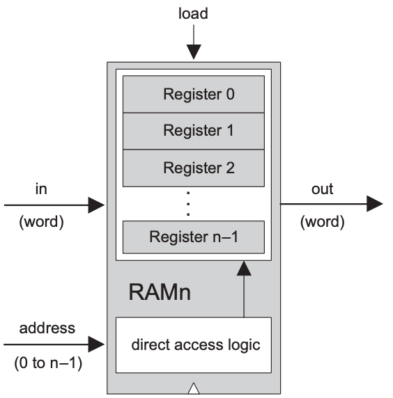
The term random access memory derives from the requirement that any randomly chosen word in the memory — irrespective of its physical location — be accessed directly, in equal speed.
This requirement can be satisfied as follows:
0 to n-1), according to which it will be accessed.n registers, we build a gate logic design that, given an address j, is capable of selecting the individual register whose address is j.In sum, a classical RAM device accepts three inputs: a data input, an address input, and a load bit. The address specifies which RAM register should be accessed in the current time unit.
In the case of a read operation (
load=0), the RAM’s output immediately emits the value of the selected register.In the case of a write operation (
load=1), the selected memory register commits to the input value in the next time unit, at which point the RAM’s output will start emitting it.
The basic design parameters of a RAM device are:
width — the width of each one of its words, and| Chip name | RAMn |
| Input | in[16], address[k], load |
| Output | out[16] |
| Function | out(t) = RAM[address(t)](t)if (load(t-1) == 1) then RAM[address(t-1)](t) = in(t-1) |
| Comment | and we will build RAM8( ),RAM64( ),RAM512( ),RAM4K( ),RAM16K( ), |
CHIP RAM8 {
    IN in[16], load, address[3];
    OUT out[16];

    PARTS:
    DMux8Way(in= load, sel= address, a= loadA, b= loadB, c= loadC, d= loadD, e= loadE, f= loadF, g= loadG, h= loadH);
    Register(in= in, load= loadA, out= out1);
    Register(in= in, load= loadB, out= out2);
    Register(in= in, load= loadC, out= out3);
    Register(in= in, load= loadD, out= out4);
    Register(in= in, load= loadE, out= out5);
    Register(in= in, load= loadF, out= out6);
    Register(in= in, load= loadG, out= out7);
    Register(in= in, load= loadH, out= out8);
    Mux8Way16(a= out1, b= out2, c= out3, d= out4, e= out5, f= out6, g= out7, h= out8, sel= address, out= out);
}
}
CHIP RAM64 {
    IN in[16], load, address[6];
    OUT out[16];

    PARTS:
    DMux8Way(in= load, sel= address[3..5], a= load1, b= load2, c= load3, d= load4, e= load5, f= load6, g= load7, h= load8);
    RAM8(in= in, load= load1, address= address[0..2], out= out1);
    RAM8(in= in, load= load2, address= address[0..2], out= out2);
    RAM8(in= in, load= load3, address= address[0..2], out= out3);
    RAM8(in= in, load= load4, address= address[0..2], out= out4);
    RAM8(in= in, load= load5, address= address[0..2], out= out5);
    RAM8(in= in, load= load6, address= address[0..2], out= out6);
    RAM8(in= in, load= load7, address= address[0..2], out= out7);
    RAM8(in= in, load= load8, address= address[0..2], out= out8);
    Mux8Way16(a= out1, b= out2, c= out3, d= out4, e= out5, f= out6, g= out7, h= out8, sel= address[3..5], out= out);
}
CHIP RAM512 {
    IN in[16], load, address[9];
    OUT out[16];

    PARTS:
    DMux8Way(in= load, sel= address[6..8], a= load1, b= load2, c= load3, d= load4, e= load5, f= load6, g= load7, h= load8);
    RAM64(in= in, load= load1, address= address[0..5], out= out1);
    RAM64(in= in, load= load2, address= address[0..5], out= out2);
    RAM64(in= in, load= load3, address= address[0..5], out= out3);
    RAM64(in= in, load= load4, address= address[0..5], out= out4);
    RAM64(in= in, load= load5, address= address[0..5], out= out5);
    RAM64(in= in, load= load6, address= address[0..5], out= out6);
    RAM64(in= in, load= load7, address= address[0..5], out= out7);
    RAM64(in= in, load= load8, address= address[0..5], out= out8);
    Mux8Way16(a= out1, b= out2, c= out3, d= out4, e= out5, f= out6, g= out7, h= out8, sel= address[6..8], out= out);

}
CHIP RAM4K {
    IN in[16], load, address[12];
    OUT out[16];

    PARTS:
    DMux8Way(in= load, sel= address[9..11], a= load1, b= load2, c= load3, d= load4, e= load5, f= load6, g= load7, h= load8);
    RAM512(in= in, load= load1, address= address[0..8], out= out1);
    RAM512(in= in, load= load2, address= address[0..8], out= out2);
    RAM512(in= in, load= load3, address= address[0..8], out= out3);
    RAM512(in= in, load= load4, address= address[0..8], out= out4);
    RAM512(in= in, load= load5, address= address[0..8], out= out5);
    RAM512(in= in, load= load6, address= address[0..8], out= out6);
    RAM512(in= in, load= load7, address= address[0..8], out= out7);
    RAM512(in= in, load= load8, address= address[0..8], out= out8);
    Mux8Way16(a= out1, b= out2, c= out3, d= out4, e= out5, f= out6, g= out7, h= out8, sel= address[9..11], out= out);

}
CHIP RAM16K {
    IN in[16], load, address[14];
    OUT out[16];

    PARTS:
    DMux8Way(in= load, sel= address[11..13], a= load1, b= load2, c= load3, d= load4, e= load5, f= load6, g= load7, h= load8);
    RAM4K(in= in, load= load1, address= address[0..11], out= out1);
    RAM4K(in= in, load= load2, address= address[0..11], out= out2);
    RAM4K(in= in, load= load3, address= address[0..11], out= out3);
    RAM4K(in= in, load= load4, address= address[0..11], out= out4);
    RAM4K(in= in, load= load5, address= address[0..11], out= out5);
    RAM4K(in= in, load= load6, address= address[0..11], out= out6);
    RAM4K(in= in, load= load7, address= address[0..11], out= out7);
    RAM4K(in= in, load= load8, address= address[0..11], out= out8);
    Mux8Way16(a= out1, b= out2, c= out3, d= out4, e= out5, f= out6, g= out7, h= out8, sel= address[11..13], out= out);

}
A out = out(t - 1) + c, where c is typically 1.
A counter chip can be implemented by combining the input/output logic of a standard register with the combinatorial logic for adding a constant.
Typically, the counter will have to be equipped with some additional functionality, such as possibilities for resetting the count to zero, loading a new counting base, or decrementing instead of incrementing.
| Chip name | Counter |
| Input | in[16], load, inc, reset |
| Output | out[16] |
| Function | if (reset(t-1) == 1) then out(t) = 0else if (load(t-1) == 1) then out(t) = in(t-1)else if (inc(t-1) == 1) then out(t) = out(t-1) + 1else out(t) = out(t-1) |
CHIP PC {
    IN in[16], reset, load, inc;
    OUT out[16];

    PARTS:
    Register(in= inRegister, load= true, out= outRegister, out= out);
    Inc16(in= outRegister, out= outInc);
    Mux16(a= outRegister, b= outInc, sel= inc, out= out1);
    Mux16(a= out1, b= in, sel= load, out= out2);
    Mux16(a= out2, b= false, sel= reset, out= inRegister);
}
Simply stated, a sequential chip is a chip that embeds one or more DFF gates, either directly or indirectly.
A
A
This chapter only focuses on the machine language and leaves the hardware details to the next chapter. To give a general description of machine languages, it's sufficient to only use three main hardware abstractions:
addition, subtraction, multiplication, division)AND, OR, NOT)load, store)jump, branch). The operands of these operations and their results/output are binary values that are read and stored in registers or selected memory locations.
A machine language is a series of coded instructions. For example, an instruction in a 16-bit computer may be 1010001100011001.
In order to figure out what this instruction means, we must know the
Since binary codes are rather cryptic, machine languages are normally specified using both 1010001100011001 may be associated with the mnemonic ADD R1, R2, R3.
Hence, a machine language instruction can be specified either directly using binary codes or indirectly using symbolic mnemonics.
We can take the symbolic abstraction one step further, and create a programming language that allows the creation of programs using symbolic commands rather than binary instructions.
This programming language is called an
The Hack computer is a
A and D. These registers can be manipulated explicitly by arithmetic and logical instructions (e.g. D=A+1, A=D&A).
The D register is used solely to store data values; while the A register is used to both store data values and memory addresses.
So, depending on the context, the contents of A can be interpreted as:Why do we overload the
Aregister with so many roles? Since Hack instructions are 16-bit wide, and since addresses are specified using 15-bits, it's impossible to pack both anoperation code and an address in one instruction. Thus, the syntax of the Hack language mandates that memory access instructions operate on an implicit memory location labeledM, for exampleD=M+1. In order to resolve this address, the convention is thatMalways refers to the memory word whose address is the current value of theAregister.That is . This implies, we must first load the address into theMis a synonym forRAM[A]Aregister before we can access the memory word at that address.This also applies to instruction memory access. To jump to a specific instruction, we must first load the address of that instruction into the
Aregister.In a nutshell, the
Aregister's value is interpreted based on how it is used in subsequent instructions.An alternative solution would be to have more registers, but this would have increased the complexity of the hardware.
The Hack language consists of two generic instructions:
The A register to a 15-bit value:
A-instruction's symbolic representation: @value (where value is a non-negative decimal number or a symbol referring to such a number).
A-instruction's binary representation is: 0value (where value is a 15-bit binary number).
The leftmost bit is the 0.
The A-instruction is used for three different purposes:
The
C-instruction's symbolic representation is: dest=comp;jump, where:
dest= is the destination register (optional),comp is the computation, and;jump is the jump condition (optional).C-instruction's binary representation is: 1 1 1 a c_1 c_2 c_3 c_4 c_5 c_6 d_1 d_2 d_3 j_1 j_2 j_3, where:
a_n & c_n specify the comp component;d_n specifies the dest component, andj_n specifies the jump component.The leftmost bit is the 1. The next two bits are not used and are set to 1.
The dest component of the C-instruction
The first and second bits specify whether to store the computed value in the A register and in the D register, respectively.
The third bit specifies whether to store the computed value in the data memory location specified by the A register.
| d1 | d2 | d3 | dest mnemonic | Destination (where to store the computed value) |
|---|---|---|---|---|
| 0 | 0 | 0 | null |
Do not store the computed value |
| 0 | 0 | 1 | M |
Store the computed value in the data memory |
| 0 | 1 | 0 | D |
Store the computed value in the D register |
| 0 | 1 | 1 | MD |
Store the computed value in the D register and in the data memory |
| 1 | 0 | 0 | A |
Store the computed value in the A register |
| 1 | 0 | 1 | AM |
Store the computed value in the A register and in the data memory |
| 1 | 1 | 0 | AD |
Store the computed value in the A register and in the D register |
| 1 | 1 | 1 | AMD |
Store the computed value in the A register, in the D register, and in the data memory |
The comp component of the C-instructionD, A, and M registers.
The a-bit specifies whether the A register or the M register should be used as the ALU's input.
And the six c-bits specifies the function to be computed.
All 7-bit comprise the comp field. While this 7-bit field can specify different possible operations, only are used in the Hack language.
| (when a=0) comp mnemonic | c1 | c2 | c3 | c4 | c5 | c6 | (when a=1) comp mnemonic |
|---|---|---|---|---|---|---|---|
0 |
1 |
0 |
1 |
0 |
1 |
0 |
|
1 |
1 |
1 |
1 |
1 |
1 |
1 |
|
-1 |
1 |
1 |
1 |
0 |
1 |
0 |
|
D |
0 |
0 |
1 |
1 |
0 |
0 |
|
A |
1 |
1 |
0 |
0 |
0 |
0 |
M |
!D |
0 |
0 |
1 |
1 |
0 |
1 |
|
!A |
1 |
1 |
0 |
0 |
0 |
1 |
!M |
-D |
0 |
0 |
1 |
1 |
1 |
1 |
|
-A |
1 |
1 |
0 |
0 |
1 |
1 |
-M |
D+1 |
0 |
1 |
1 |
1 |
1 |
1 |
|
A+1 |
1 |
1 |
0 |
1 |
1 |
1 |
M+1 |
D-1 |
0 |
0 |
1 |
1 |
1 |
0 |
|
A-1 |
1 |
1 |
0 |
0 |
1 |
0 |
M-1 |
D+A |
0 |
0 |
0 |
0 |
1 |
0 |
D+M |
D-A |
0 |
1 |
0 |
0 |
1 |
1 |
D-M |
A-D |
0 |
0 |
0 |
1 |
1 |
1 |
M-D |
D&A |
0 |
0 |
0 |
0 |
0 |
0 |
D&M |
D|A |
0 |
1 |
0 |
1 |
0 |
1 |
D|M |
The jump component of the C-instructionj-bits of the jump component and the ALU's output value.
It is a 3-bit field that can specify one of different jump conditions.
j1 (out < 0) |
j2 (out = 0) |
j3 (out > 0) |
jump mnemonic | Effect |
|---|---|---|---|---|
0 |
0 |
0 |
null |
No jump (this is the default, it simply proceeds to the next instruction) |
0 |
0 |
1 |
JGT |
Jump if out > 0 |
0 |
1 |
0 |
JEQ |
Jump if out = 0 |
0 |
1 |
1 |
JGE |
Jump if out >= 0 |
1 |
0 |
0 |
JLT |
Jump if out < 0 |
1 |
0 |
1 |
JNE |
Jump if out != 0 |
1 |
1 |
0 |
JLE |
Jump if out <= 0 |
1 |
1 |
1 |
JMP |
Jump unconditionally |
The JMP is used as 0;JMP. This is because the C-instruction syntax requires that we always effect some computation, we instruct the ALU to compute (an arbitrary choice), which is ignored.
Example: We want the computer to increment the value of DataMemory[7] by and to also store the result in the D register. This can be achieved with the following instructions:
 0000 0000 0000 0111 // @7
 1111 1101 1101 1000 // MD=M+1
Assembly commands can refer to memory addresses using either constants or symbols. Symbols are introduced into assembly programs in the following three ways:
R0 to R15 refer to RAM addresses 0 to 15, respectively.SP, LCL, ARG, THIS, and THAT refer to RAM addresses 0, 1, 2, 3, and 4, respectively.SCREEN and KBD refer to RAM addresses 16384 (0x4000) and 24576 (0x6000), respectively, which are the base addresses of the screen and
keyboard memory maps.(Xxx). This directive defines the symbol
Xxx to refer to the ROM address holding the next command in the program.Xxx that appears in an assembly program without being predefined or declared as a label is treated as a variable.
The assembler allocates a unique RAM address for each appearance of such a symbol and replaces the symbol with its RAM address in the assembly program.
The instruction is of the form @value, where value is a 15-bit (non-numerical) constant.The Hack platform can be connected to two peripheral devices:
The Hack computer includes a black-and-white screen organized as rows of pixels per row.
The screen’s contents are represented by an 8K memory map that starts at RAM address ( ).
Each row in the physical screen, starting at the screen’s top left corner, is represented in the RAM by consecutive 16-bit words.
Thus, the pixel at row r from the top and column c from the left is mapped on the c%16 bit (counting from LSB to MSB) of the word located at RAM[16384 + r * 32 + c/16].
To write or read a pixel of the physical screen, one reads or writes the corresponding bit in the RAM-resident memory map (1 = black, 0 = white).
Example:
// Draw a single black dot at the screen's top left corner:
@SCREEN // Set the A register to point to the memory
       // word that is mapped to the 16 left-most
      // pixels of the top row of the screen.
M=1 // Blacken the left-most pixel.
The Hack computer interfaces with the physical keyboard via a single-word memory map located in RAM address ( ).
Whenever a key is pressed on the physical keyboard, its 16-bit ASCII code appears in RAM[24576].
When no key is pressed, the code 0 appears in this location.
In addition to the usual ASCII codes, the Hack keyboard recognizes the keys shown below.
| Key pressed | Code |
|---|---|
| newline | 128 |
| backspace | 129 |
| left arrow | 130 |
| up arrow | 131 |
| right arrow | 132 |
| down arrow | 133 |
| home | 134 |
| end | 135 |
| page up | 136 |
| page down | 137 |
| insert | 138 |
| delete | 139 |
| esc | 140 |
| f1-f2 | 141-152 |
@R2
M=0
@count
M=0
(loop_start)
@R1
D=M
@count
D=D-M
@loop_end
D;JEQ
@R0
D=M
@R2
M=D+M
@count
M=M+1
@loop_start
0;JMP
(loop_end)
@loop_end
0;JMP
(keyboard_loop_start)
@KBD
D=M
@on_keyboard_input
// The D register will be positive if a key is pressed
D;JGT

// Set fill color to white (i.e. "0").
@fill_color
M=0
@SCREEN
D=M
// Jump to start if screen is already filled with white (i.e. "0").
@keyboard_loop_start
D;JEQ
// Jump to paint loop
@paint_loop_init
0;JMP

(on_keyboard_input)
// Set fill color to black (i.e. "-1").
@fill_color
M=-1
@SCREEN
D=M
// Jump to start if screen is already filled with black (i.e. "-1").
@keyboard_loop_start
D;JLT
// Else, continue as normal

(paint_loop_init)
@R1
M=0
(paint_loop_start)
@SCREEN
D=A
@R1
A=D+M

// Temporarily store the screen address in the D register, then store it in a "temp" variable.
// Next, set the D register to the value of the "fill_color" variable.
// Finally, read the screen address from the "temp" variable.
// All this gymnastics allows us to store the fill color in the D register.
D=A
@temp
M=D
@fill_color
D=M
@temp
A=M
M=D

@R1
MD=M+1
// The screen has 8kb size, so we repeat this loop for the entire size to fill the screen.
@8192
D=A-D
@paint_loop_start
D;JGT
@keyboard_loop_start
0;JMP
The computer is based on a
The
At the heart of this architecture lies the

A related stored program computer architecture is the

The CPU operation can be described as a repeated loop (aka
(3) and (4) are based on the fetched instruction which tells the CPU:
The CPU executes these tasks using three main hardware elements:
The first two elements were already introduced in the previous chapters.
A computer instruction is represented as a binary code, typically 16, 32, or 64 bits wide.
Before such an instruction can be
The instruction decoding is done by some
The set of registers used by the Hack computer are:
D)D register is used to speed up operations.A)A register's value can be read directly as a data value.PC)The Hack computer is a 16-bit machine based on the Harvard architecture, designed to execute instructions written in the Hack machine language.
The Hack CPU interface:
CHIP CPU

IN
    instruction[16], //	Instruction	to	execute.
    inM[16], //	Value of Mem[A], the instruction’s M input
    reset; // Signals whether to continue executing	the	current	program	(reset==0) or restart the current program (reset==1).

OUT
    outM[16], // Value to write to Mem[addressM], the instruction’s M output
    addressM[15], // In	which address to write?
    writeM,	// Write to the Memory?
    pc[15];	// Address of next instruction
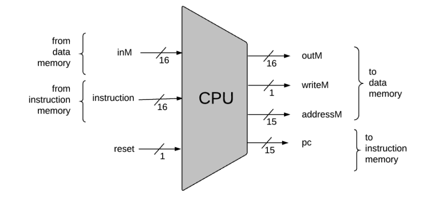
Key points:
0 opcode) that the instruction represents into the A register.0, any value may appear in outM).0, the CPU uses the ALU output and the jump directive specified by the instruction to compute the address of the next instruction, and emits this address to the pc output.1, the CPU sets pc to 0.The Hack instruction memory interface:
CHIP ROM32K

IN
    address[15];

OUT
    out[16];
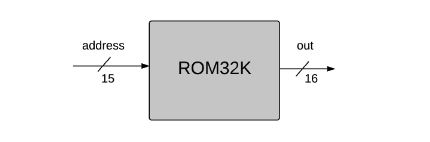
Key points:
out = ROM32K[address].The Hack data memory interface:
CHIP Memory

IN
    in[16],	load,	address[15];

OUT
    out[16];
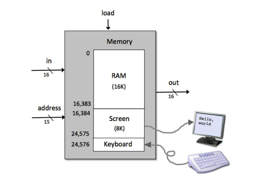
Key points:
out(t) = Mem[address(t)](t)if load(t) then Mem[address(t)](t+1) = in(t)16K + 8K + 1 words of the address space are used.0x0000 - 0x5FFF: accessing an address in this range results in accessing the RAM.0x4000 - 0x5FFF: accessing an address in this range results in accessing the Screen.0x6000: accessing this address results in accessing the Keyboard.>= 0x6000: accessing an address in this range is invalid.The interface of the topmost chip in the Hack hardware platform, named Computer:
CHIP Computer

IN
    reset;
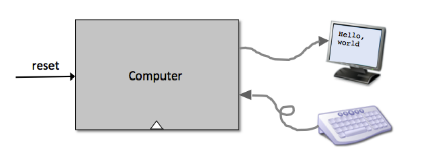
Key points:
reset==0, the program stored in the computer's ROM executes.reset==1, the execution of the program restarts.The Hack keyboard chip interface:
CHIP Keyboard

OUT
    out[16]; //	The	scan-code of the pressed key, or 0 if no key is currently pressed.
Keypoint:
0 if no key is pressed.The Hack screen chip interface:
CHIP Screen

IN
    in[16], // what to write
    address[13]; //	where to write (or read)
    load, // write-enable bit

OUT
    out[16]; //	Screen value at the given address
Keypoint:
out(t) = Screen[address(t)](t)if load(t) then Screen[address(t)](t+1) = in(t)c % 16 bit (counting from LSB to MSB) of the 16-bit word stored in Screen[r * 32 + c / 16].All the chips needed to build the Hack CPU have been built in the previous chapters, the key question is how to arrange and connect them in a way that effects the desired CPU operation.
The architecture shown below is used to perform three classical CPU tasks:
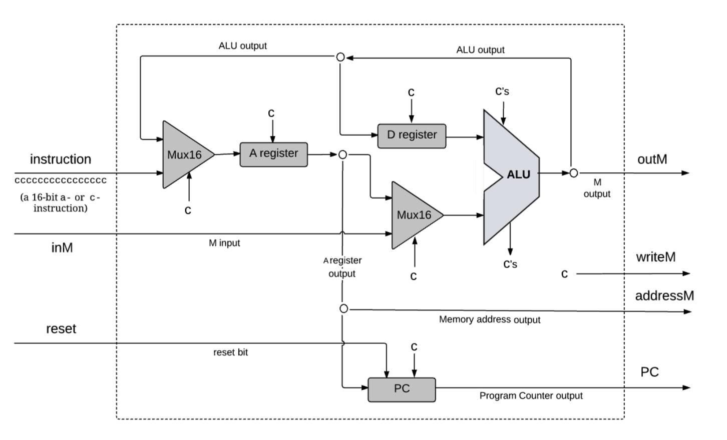 Every
Every c symbol entering a chip-part stands for some control bit, extracted from the instruction.
In the case of the ALU, the c's input stands for the 6 control bits that instruct the ALU what to compute, and the c's
output stands for its zr and ng outputs.
Taken together, the distributed behaviors that these control bits effect throughout the CPU architecture end up executing the instruction.
// This file is part of www.nand2tetris.org
// and the book "The Elements of Computing Systems"
// by Nisan and Schocken, MIT Press.
// File name: projects/5/CPU.hdl
/**
 * The Hack Central Processing unit (CPU).
 * Parses the binary code in the instruction input and executes it according to the
 * Hack machine language specification. In the case of a C-instruction, computes the
 * function specified by the instruction. If the instruction specifies to read a memory
 * value, the inM input is expected to contain this value. If the instruction specifies
 * to write a value to the memory, sets the outM output to this value, sets the addressM
 * output to the target address, and asserts the writeM output (when writeM = 0, any
 * value may appear in outM).
 * If the reset input is 0, computes the address of the next instruction and sets the
 * pc output to that value. If the reset input is 1, sets pc to 0.
 * Note: The outM and writeM outputs are combinational: they are affected by the
 * instruction's execution during the current cycle. The addressM and pc outputs are
 * clocked: although they are affected by the instruction's execution, they commit to
 * their new values only in the next cycle.
 */
CHIP CPU {

    IN  inM[16],         // M value input  (M = contents of RAM[A])
        instruction[16], // Instruction for execution
        reset;           // Signals whether to re-start the current
                         // program (reset==1) or continue executing
                         // the current program (reset==0).

    OUT outM[16],        // M value output
        writeM,          // Write to M?
        addressM[15],    // Address in data memory (of M)
        pc[15];          // address of next instruction

    PARTS:
    // Negate the opCode.
    Not(in= instruction[15], out= notOpCode);
    // If opCode == 0, we route the instruction into the A register. Else, we route the ALU input.
    Mux16(a= outputOfALU, b= instruction, sel= notOpCode, out= inputToA);
    // The A register is enabled for writing if we have an A-instruction or a C-instruction with the d_1 control bit asserted.
    Or(a= notOpCode, b= instruction[5], out= writeToA);
    ARegister(in= inputToA, load= writeToA, out= outputOfA, out[0..14]=addressM);

    // Only select M, if we have an C-instruction and the a-bit is asserted
    And(a= instruction[15], b= instruction[12], out= controlAOrM);
    Mux16(a= outputOfA, b= inM, sel= controlAOrM, out= AOrM);
    // Use the ALU.
    ALU(x= outputOfD, y= AOrM, zx= instruction[11], nx= instruction[10], zy= instruction[9], ny= instruction[8], f= instruction[7], no= instruction[6], out= outputOfALU, out = outM, zr= isAluOutputZero, ng= isAluOutputNegative);

    // Only write to the D register, if we have a C-instruction AND the d_2 bit is asserted.
    And(a= instruction[15], b= instruction[4], out= writeToD);
    DRegister(in= outputOfALU, load= writeToD, out= outputOfD);

    // Only set writeM to true, if we have a C-instruction and the d_1 bit is asserted.
    And(a= instruction[15], b= instruction[3], out= controlWriteM);
    Mux(a= false, b= true, sel= controlWriteM, out= writeM);

    // Derive if ALU output is positive (i.e, it's not negative or zero)
    Or(a= isAluOutputNegative, b= isAluOutputZero, out= isAluOutputNegativeOrZero);
    Not(in= isAluOutputNegativeOrZero, out= isAluOutputPositive);

    // Check j_1 against ALU output is negative bit.
    And(a= instruction[2], b= isAluOutputNegative, out= jumpCauseNegative);
    // Check j_2 against ALU output is zero bit.
    And(a= instruction[1], b= isAluOutputZero, out= jumpCauseZero);
    // Check j_3 against ALU output is positive bit.
    And(a= instruction[0], b= isAluOutputPositive, out= jumpCausePositive);

    // Combine: We jump if we have a C-instruction and any of the jump predicates matches.
    Or(a= jumpCauseNegative, b= jumpCauseZero, out= jumpIntermediate);
    Or(a= jumpIntermediate, b= jumpCausePositive, out= jumpIntermediate2);
    And(a= instruction[15], b= jumpIntermediate2, out= controlJump);

    PC(in= outputOfA, load= controlJump, inc= true, reset= reset, out[0..14]= pc);
}
// This file is part of www.nand2tetris.org
// and the book "The Elements of Computing Systems"
// by Nisan and Schocken, MIT Press.
// File name: projects/5/Memory.hdl
/**
 * The complete address space of the Hack computer's memory,
 * including RAM and memory-mapped I/O.
 * The chip facilitates read and write operations, as follows:
 *     Read:  out(t) = Memory[address(t)](t)
 *     Write: if load(t-1) then Memory[address(t-1)](t) = in(t-1)
 * In words: the chip always outputs the value stored at the memory
 * location specified by address. If load=1, the in value is loaded
 * into the memory location specified by address. This value becomes
 * available through the out output from the next time step onward.
 * Address space rules:
 * Only the upper 16K+8K+1 words of the Memory chip are used.
 * Access to address>0x6000 is invalid and reads 0. Access to any address
 * in the range 0x4000-0x5FFF results in accessing the screen memory
 * map. Access to address 0x6000 results in accessing the keyboard
 * memory map. The behavior in these addresses is described in the Screen
 * and Keyboard chip specifications given in the lectures and the book.
 */
CHIP Memory {
    IN in[16], load, address[15];
    OUT out[16];

    PARTS:


    // 0000 000 RAM start
    // 0011 FFF RAM end
    // 0100 000 Screen start
    // 0101 FFF Screen end
    // 0110 000 Keyboard

    DMux4Way(
        in=load,
        sel=address[13..14],
        a=loadRam1,
        b=loadRam2,
        c=loadScreen,
        d=ignoredLoadKeyboard
    );
	Or(a=loadRam1, b=loadRam2, out=loadRam);

    RAM16K(in=in, load=loadRam, address=address[0..13], out=ramOut);
    Screen(in=in, load=loadScreen, address=address[0..12], out=screenOut);
    Keyboard(out=keyboardOut);

    Mux4Way16(
        a=ramOut,
        b=ramOut,
        c=screenOut,
        d=keyboardOut,
        sel=address[13..14],
        out=out
    );
}
// This file is part of www.nand2tetris.org
// and the book "The Elements of Computing Systems"
// by Nisan and Schocken, MIT Press.
// File name: projects/5/Computer.hdl
/**
 * The Hack computer, consisting of CPU, ROM and RAM.
 * When reset = 0, the program stored in the ROM executes.
 * When reset = 1, the program's execution restarts.
 * Thus, to start running the currently loaded program,
 * set reset to 1, and then set it to 0.
 * From this point onwards, the user is at the mercy of the software.
 * Depending on the program's code, and whether the code is correct,
 * the screen may show some output, the user may be expected to enter
 * some input using the keyboard, or the program may do some procerssing.
 */
CHIP Computer {

    IN reset;

    PARTS:

    Memory(
        in= cpuMemoryOut,
        load= writeCpuMemoryOut,
        address= cpuMemoryOutAddress,
        out= memoryOut
    );

    ROM32K(
        address= programCounter,
        out= instruction
    );

    CPU(
        inM= memoryOut,
        instruction= instruction,
        reset= reset,
        outM= cpuMemoryOut,
        writeM= writeCpuMemoryOut,
        addressM= cpuMemoryOutAddress,
        pc= programCounter
    );
}
A
To improve readability and ease of programming, we use a symbolic language called load, R3, and 7, translates each field into its equivalent binary code,
and finally assembles the generated bits into a binary instruction that can be executed by the hardware.
An
(xxx), where xxx is a symbolic label.// is considered a comment and is ignored.Symbols in Hack assembly programs fall into three categories:
R0, R1, …, R15 stand for 0, 1, … 15, respectively.SP, LCL, ARG, THIS, THAT stand for 0, 1, 2, 3, 4, respectively.SCREEN and KBD stand for 16384 and 24576, respectively.(xxx) defines the symbol xxx to refer to the location in the
Hack ROM holding the next instruction in the program. A label symbol can be defined once and can be used anywhere in
the assembly program, even before the line in which it is defined.xxx appearing in an assembly program that is not predefined and is not
defined elsewhere by a label declaration (xxx) is treated as a variable.
Variables are mapped to consecutive RAM locations as they are first encountered, starting at RAM address 16Assembly programs can use symbolic references to memory addresses. An assembler handles this by using a
See the project for implementation details.
Solution code is on GitHub.
Before a high-level program can run on a target computer, it must be translated into the computer’s machine language.
Modern compilers typically translate high-level programs into an intermediate code designed to run on an abstract computer called a
This chapter presents a typical
Traditional
The design of an effective VM language strikes a good balance between high-level and low-level languages.
The VM commands should be sufficiently “high” so that the VM code generated by the compiler will be reasonably elegant and well structured. At the same time, the VM commands should be sufficiently “low” so that the machine code generated from them by the VM translators will be tight and efficient.
One way to satisfy these somewhat conflicting requirements is to base the interim VM language on an abstract architecture called a
The centerpiece of the stack model is an
The push/pop combination leads to a
Our VM abstraction consists of two data structures:
Arithmetic and boolean expressions can be represented and evaluated by elementary operations on a stack.
In a stack machine, the generic binary operation x op y is carried out as follows:
x and y are popped off the stack.x op y is computedThe generic unary operation op x is carried out in a similar fashion.
From the stack’s perspective, each arithmetic or logical operation has the net impact of replacing the operation’s operands with the operation’s result, without affecting the rest of the stack.
A typical object-based language have variables at various scopes:
Variable scopes are represented in the virtual machine as virtual memory segments and variables are stored as entries in them:
| Segment | Role |
|---|---|
| argument | Represents the function’s argument. |
| local | Represents the function’s local variables. |
| static | Represents the static variables seen by the function. |
| constant | Represents the constant values 0, 1, 2, 3, …, 32767. |
| this | Described in later chapters. |
| that | Described in later chapters. |
| pointer | Described in later chapters. |
| temp | Described in later chapters. |
VM commands access all the memory segments in exactly the same way: by using the segment name followed by a non-negative index.
The compiler maps the first, second, third, … static variable found in the high-level program onto static 0, static 1, static 2, and so on. The other variable kinds are mapped similarly into their respective segments.
For example, if the local variable x and the field y have been mapped on local 1 and this 3, respectively, then a high-level statement like let x = y will be translated by the compiler into push this 3 and pop local 1.
Our VM model is stack-based: all the VM operations take their operands from, and store their results on, the stack.
A VM program is a sequence of VM commands that fall into four categories:
In this chapter we focus on the arithmetic-logical and push/pop commands.
// are considered comments and are ignored. Blank lines are permitted and are ignored.push segment index: Pushes the value of segment[index] onto the stack.pop segment index: Pops the top stack value and stores it in segment[index].add, sub, neg (unary).eq, gt, lt.and, or, not (unary).The commands add, sub, eq, gt, lt, and, and or have neg and not commands have
The abstract VM described so far must be implemented on a host machine to actually run. The implementation option chosen by the project is a
Writing a VM translator entails two main tasks:
We can represent the VM’s stack using a designated memory block in the host RAM. The lower end of this RAM block will be a fixed base address, and its higher end will change as the stack grows and shrinks.
Thus, given a fixed stackBase address, we can manage the stack by keeping track of a single variable: a SP to stackBase.
Let's assume that the stackBase address is 256 in the Hack computer RAM. In that case, the VM translator can start by generating assembly code that realizes SP=256, that is:
@256
D = A
@SP
M = D
From this point onward, the VM translator can handle each push x and pop x command by generating assembly code that realizes the operations RAM[sp++] = x and x = RAM[--sp], respectively.
For the VM arithmetic-logical commands, conveniently, all the commands share exactly the same access logic: popping the command’s operands off the stack, carrying out a simple calculation, and pushing the result onto the stack.
In principle, the most important thing is correctly and efficiently implementing the VM abstraction on a hardware platform (i.e. The actual implementation details are irrelevant). Nevertheless, VM architects normally publish basic implementation guidelines, known as
A FileName.vm. The VM translator should read each line in the file, treat it as a VM command, and translate it into one or more instructions written in the Hack assembly language stored in a text file named FileName.asm.
The VM abstraction has only one data type: a signed integer. This type is implemented on the Hack platform as a two’s complement 16-bit value. The VM Boolean values true and false are represented as -1 and 0 respectively.
The host Hack RAM consists of 32K 16-bit words. VM implementations should use the top of this address space as follows:
| RAM address | Usage |
|---|---|
| 0-15 | Sixteen virtual registers (described in the other table below) |
| 16-255 | Static variables |
| 256-2047 | Stack |
| Name | Location | Usage |
|---|---|---|
| SP | RAM[0] | Points to the memory address just following the memory address containing the topmost stack value. |
| LCL | RAM[1] | Points to the base memory address of the current VM function’s local segment. |
| ARG | RAM[2] | Points to the base memory address of the current VM function’s argument segment. |
| THIS | RAM[3] | Points to the base memory address of the current VM function’s this segment. |
| THAT | RAM[4] | Points to the base memory address of the current VM function’s that segment. |
| TEMP | RAM[5-12] | A general-purpose segment. |
| R13, R14, R15 | RAM[13-15] | If the assembly code generated by the VM translator needs variables, it can use these registers. |
Assume that
SP,ARG,LCL,THIS, andTHAThave been already initialized to some sensible addresses in the host RAM.
Note that VM implementations never see these addresses anyway. Rather, they manipulate them symbolically, using the pointer names. For example, suppose we want to push the value of the D register onto the stack. This operation can be implemented using the logic which can be expressed in Hack assembly as:
@SP // Sets the A register to address pointed to by SP (the stack pointer).
A = M // Basically, SP is amemory address on the RAM, and the value at RAM[SP] is also an address on the RAM. This instruction sets the A register to the value at RAM[SP].
M = D // Sets RAM[RAM[SP]] to the value of the D register.
@SP // Sets the A register to address pointed to by SP (the stack pointer).
M = M + 1 // Increments the value at RAM[SP] by 1 (i.e. increments the stack pointer).
LCL, ARG, THIS, and THAT, respectively. Therefore, any access to the i-th entry of a virtual segment (in the context of a VM “push / pop segmentName i” command) should be translated into assembly code that accesses address (base + i) in the RAM.3 and 4. Recall that these RAM locations are also called, respectively, THIS and THAT. Thus, the semantics of the pointer segment is as follows: Any access to pointer 0 should result in accessing the THIS pointer, and any access to pointer 1 should result in accessing the THAT pointer. For example, pop pointer 0 should set THIS to the popped value, and push pointer 1 should push onto the stack the current value of THAT.temp i, where i varies from 0 to 7, should be translated into assembly code that accesses RAM location 5 + i.constant i by simply supplying the constant i.16 to 255 of the host RAM. The VM translator can realize this mapping automatically, as follows:static i in a VM program stored in file Foo.vm can be translated to the assembly symbol Foo.i.16.16 and onward, in the order in which they appear in the VM code.push constant 100, push constant 200, pop static 5, pop static 2. The translation scheme described above will cause static 5 and static 2 to be mapped on RAM addresses 16 and 17, respectively.FileName.i symbols have unique prefix file names.256, the implementation limits the number of static variables in a Jack program to .One relatively simple way to implement a virtual machine is to write a high-level program (called a
VM emulator ) that represents the stack and the memory segments and implements all the VM commands using high-level programming.
Solution code is on GitHub.
🎯 Objective: In this chapter we’ll learn how to use and implement the VM’s branching commands and function commands.
This chapter shows how the simple
The default flow of computer programs is sequential, executing one command after the other. This sequential flow can be redirected by
In low-level programming, branching is accomplished by goto destination commands. The destination specification can take several forms:
The VM language supports two forms of branching:
goto label command, which means: jump to execute the command just after the label symbol command in the code.if-goto label command, whose semantics is:Any flow of control structure found in high-level programming languages can be realized using our (rather minimal set of) VM logical and branching commands.
Function calls and primitive commands share a
push x
push y
add
push 3
call power
Both operations require:
The term
During run-time, each function call must be executed independently of all the other calls and maintain its own stack, local variables, and argument variables. The local and argument variables of a function are temporary with a lifetime that spans the function’s execution.
Although the function calling chain may be arbitrarily deep as well as recursive, at any given point in time only one function executes at the chain’s end, while all the other functions up the calling chain are waiting for it to return. This call-and-return logic has a linear nature that makes the problem of implementing functions tractable. This Last-In-First-Out processing model lends itself perfectly to the stack data structure, which is also LIFO.
There are two problems that must be solved to implement function calling and returning:
SP before the callee starts executing and restore it when the callee returns.LCL, ARG, THIS, and THAT refer to
the base RAM addresses of the local, argument, this, and that segments of the current function.
To put these segments on hold, we can push their pointers onto the stack and restore them when the callee returns.The term
We see that the same data structure is used to hold both the working stacks and the frames of all the functions up the calling chain.
The
nArgs is the number of arguments required by the function to be called (nArgs onto the stack.call callee command.local, argument, this, and that virtual registers onto the stack.argument segment is initialized with the argument values passed by the argument virtual register to SP - nArgs - callerFrameSize,
where callerFrameSize is 5 in our case (composed of return address, LCL, ARG, THIS, THAT).local virtual register is set to SP. This will be used in the static segment may have changed and the temp segment is undefined.The
function functionName nVars command.LCL was set by the SP,
so we simply achieve this by repeating pop constant 0 for nVars (the number of local variables of the this, that, pointer, and temp are undefined upon entry.argument 0 was.SP is set to one above that position. This effectively frees the global stack area below the new value of SP.label labelName: Labels the current location in the function’s code. Only labeled locations can be jumped to. The scope of the label is the function in which it is defined. The label is a string composed of any sequence of letters, digits, underscore (_), dot (.), and colon (:) that does not begin with a digit. The label command can be located anywhere in the function, before or after the goto commands that refer to it.goto labelName: Effects an unconditional goto operation, causing execution to continue from the location marked by the label. The goto command and the labeled jump destination must be located in the same function.if-goto labelName: Effects a conditional goto operation. The stack’s topmost value is popped; if the value is not zero, execution continues from the location marked by the label; otherwise, execution continues from the next command in the program. The if-goto command and the labeled jump destination must be located in the same function.function functionName nVars: Marks the beginning of a function named functionName. The command informs that the function has nVars local variables.call functionName nArgs: Calls the named function. The command informs that nArgs arguments have been pushed onto the stack before the call.return: Transfers execution to the command just following the call command in the code of the function that called the current function.The scope of VM function names is global: all the VM functions in all the vm files in the program folder see each other
and may call each other using the unique and fully qualified function name FileName.functionName.
One file in any Jack program must be named Main.jack, and one function in this file must be named main,
which is the
Sys.init,
which is part of the operating system.Sys.init is programmed to call Main.main.The output of the source.asm.
If source is a folder name, the single .asm file contains the translation of all the functions in all the .vm files in the folder, one after the other.
Solution code is on GitHub.
Jack is a simple high-level object-based language. It’s it inspired from Java, with simpler syntax and no support for inheritance.
Jack comes with a standard class library (AKA the Jack OS), which extends the basic language with various abstractions and services. The OS consists of eight classes:
| OS class | Services |
|---|---|
| Array | Array representation and manipulation: new(int), dispose, ... |
| Math | Common mathematical functions: max(int, int), sqrt(int), ... |
| Memory | Facilitates access to the host RAM: alloc(int), deAlloc(Array), peek(int), poke(int, int), .... |
| Output | Facilitates text output to the screen: printString(string), printInt(int), println, ... |
| Screen | Facilitates graphics output to the screen: setColor(boolean), drawPixel(int, int), drawLine(int, int, int, int), ... |
| Keyboard | Facilitates input from the keyboard: readLine(String), readInt(String), ... |
| String | String representation and manipulation: length(), charAt(int), ... |
| Sys | Facilitates execution-related services: halt(), wait(int), ... |
Note: I quickly went through this chapter without doing its exercises because the Jack language is very similar to Java, which I'm already familiar with. I focused only on familiarizing with the places where the Jack language differs from Java. I am not interested in gaining an intimate knowledge of Jack, but rather learning the bare minimum to be able to write the compiler in the coming chapters.
A
Compilation consists of two main stages:
The syntax analysis stage is divided two sub-stages:
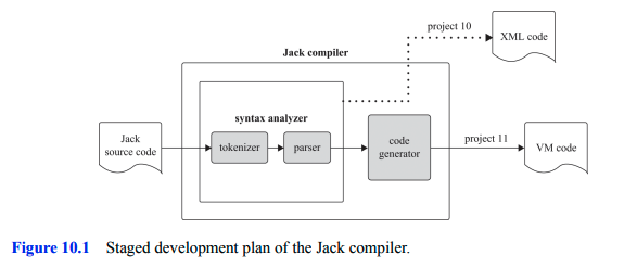
Each programming language specification includes the types of tokens, or words, that the language recognizes. Jack has the following token types:
class, constructor, function, method, field, static, var, int, char, boolean, void, true, false, null, this, let, do, if, else, while, return.{, }, (, ), [, ], ., ,, ;, +, -, *, /, &, |, <, >, =, ~.The tokens defined by these lexical categories are referred to as the
Once a program has been tokenized, the tokens, rather than the characters, are viewed as its basic atoms.
The second stage of syntax analysis is
The structured statements are called
*: Zero or more occurrences. e.g. x* means x appears zero or more times.?: Zero or one occurrence. e.g. x? means x appears zero or one time.|: Alternation. e.g. x | y means either x or y.( and ): Grouping grammar elements to be treated as a single grammatical element. e.g. (x | y) z means either x z or y z.For example, the rule "
ifStatement: 'if ' '( 'expression ') ' '{ 'statements '} '" stipulates that every valid instance of anifStatementmust begin with the tokenif , followed by the token( , followed by a valid instance of anexpression (defined elsewhere in the grammar), followed by the token) , followed by the token{ , followed by a valid instance of statements (defined elsewhere in the grammar), followed by the token} .
The Jack language includes five types of terminal elements (tokens):
class, constructor, function, method, field, static, var, int, char, boolean, void, true, false, null, this, let, do, if, else, while, return.{, }, (, ), [, ], ., ,, ;, +, -, *, /, &, |, <, >, =, ~.A Jack program is a collection of classes, each appearing in a separate file. The compilation unit is a class. A class is a sequence of tokens, as follows:
class: 'class' className '{' classVarDec* subroutineDec* '}'classVarDec: ('static' | 'field') type varName (',' varName)* ';'type: 'int' | 'char' | 'boolean' | classNamesubroutineDec: ('constructor' | 'function' | 'method') ('void' | type) subroutineName '(' parameterList ')' subroutineBodyparameterList: ((type varName) (',' type varName)*)?subroutineBody: '{' varDec* statements '}'varDec: 'var' type varName (',' varName)* ';'className: identifiersubroutineName: identifiervarName: identifierstatements: statement*statement: letStatement | ifStatement | whileStatement | doStatement | returnStatementletStatement: 'let' varName ('[' expression ']')? '=' expression ';';ifStatement: 'if' '(' expression ')' '{' statements '}' ('else' '{' statements '}')?whileStatement: 'while' '(' expression ')' '{' statements '}'doStatement: 'do' subroutineCall ';'returnStatement: 'return' expression? ';'expression: term (op term)*term: integerConstant | stringConstant | keywordConstant | varName | varName '[' expression ']' | subroutineCall | '(' expression ')' | unaryOp termsubroutineCall: subroutineName '(' expressionList ')' | (className | varName) '.' subroutineName '(' expressionList ')'expressionList: (expression (',' expression)*)?op: '+' | '-' | '*' | '/' | '&' | '|' | '<' | '>' | '='unaryOp: '-' | '~'keywordConstant: 'true' | 'false' | 'null' | 'this'Grammars are inherently recursive.
if (x<0){if(y > 0){...}}
The grammar can be used to parse the above code as follows:
ifStatement: '(x<0).if(y>0){...} which is an ifStatement.The parser produces an exact correspondence between the given input, on the one hand, and the syntactic patterns admitted by the grammar rules, on the other.
The correspondence can be represented by a data structure called a
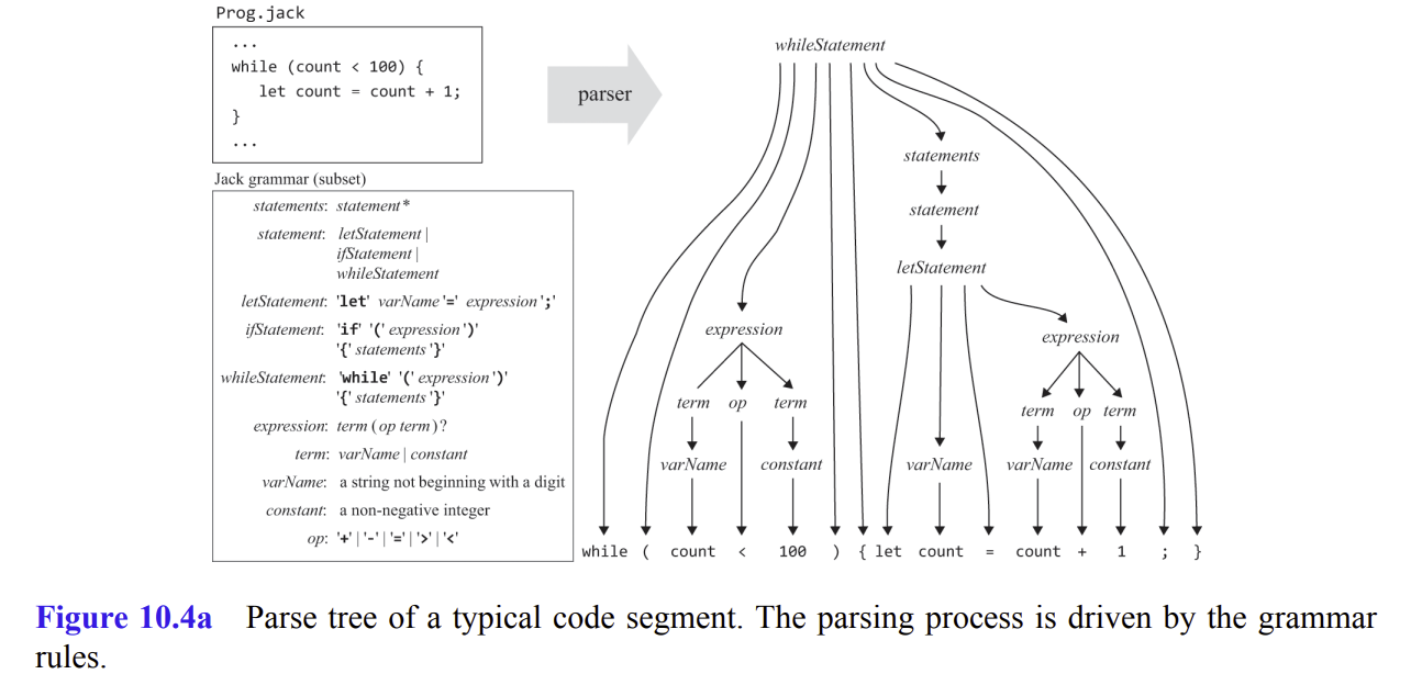
A parser is an agent that operates according to a given grammar. The parser accepts as input a stream of tokens and attempts to produce as output the parse tree associated with the given input. In our case, the input is expected to be structured according to the Jack grammar, and the output is written in XML.
There are several algorithms for constructing parse trees. The top-down approach, also known as
For every nontrivial rule in the grammar, we equip the parser program with a routine designed to parse the input according to that rule.
For example, the grammar listed previously can be implemented using a set of routines named:
compileStatement, compileStatements,compileLet,compileIf,compileExpression, and so on.The parsing logic of each compileXXX routine should follow the syntactic pattern specified by the right side of the XXX rule.
For example, according to our scheme, the whileStatement rule will be implemented by a parsing routine named compileWhile.
This routine should realize the left-to-right derivation logic specified by the pattern
"'compileWhile routine:
// This routine implements the rule whileStatement: 'while' '(' expression ')' '{' statements '}'.
// Should be called if the current token is 'while'.
compileWhile():
    print("<whileStatement>")
    process("while")
    process("(")
    compileExpression()
    process(")")
    process("{")
    compileStatements()
    process("}")
    print("</whileStatement>")

// A helper routine that handles the current token, and advances to get the next token.
process(token):
    if (currentToken == token):
        printXMLToken(currentToken)
        currentToken = tokenizer.advance()
    else:
        error("Syntax error: Expected token " + token + " but got " + currentToken)
This parsing process will continue until the expression and statements parts of the while statement have been fully parsed.
Each compileXXX routine follow the same contract:
XXX,Recursive parsing algorithms are simple and elegant. Jack's grammar is simple, only requiring a
Grammars that have this lingual property are called
For example:
let, we know that we have a letStatement;while, we know that we have a whileStatement,Solution code is on GitHub.
The syntax analyzer was built in order to develop, and demonstrate, a capability for parsing high-level programs into their underlying syntactical elements. In this chapter we’ll morph the analyzer into a full-scale compiler: a program that converts the parsed elements into VM commands designed to execute on the abstract virtual machine described in chapters 7-8. This approach follows the modular analysis-synthesis paradigm that informs the construction of well-designed compilers. It also captures the very essence of translating text from one language to another: first, one uses the source language’s syntax for analyzing the source text and figuring out its underlying semantics, that is, what the text seeks to say; next, one re-expresses the parsed semantics using the syntax of the target language.
One of the basic tasks of compilers is mapping the variables declared in the source high-level program onto the host RAM of the target platform. Thus, every Jack variable, including pointer variables holding 16-bit address values, can be mapped on exactly one word in memory.
The second challenge faced by compilers is that variables of different kinds have different life cycles.
In our two-tier compiler architecture, memory allocation and de-allocation are delegated to the VM level. All we have to do now is map:
The subsequent mapping of the virtual memory segments on the host RAM, as well as the intricate management of their run-time life cycles, are completely taken care of by the VM implementation.
Recall that this implementation was not achieved easily: we had to work hard to generate assembly code that dynamically maps the virtual memory segments on the host RAM as a side effect of realizing the function call-and-return protocol. Now we can reap the benefits of this effort: the only thing required from the compiler is mapping the high-level variables onto the virtual memory segments. All the subsequent gory details associated with managing these segments on the RAM will be handled by the VM implementation.
In a two-tier compilation model, the handling of variables can be reduced to mapping high-level variables on virtual memory segments and using this mapping, as needed, throughout code generation. These tasks can be readily managed using a classical abstraction known as a symbol table.
Solution code is on GitHub.
// Return x * y, where x, y >= 0
multiply(x, y):
    sum = 0
    shiftedX = x

    for i = 0 ... n - 1 do
        if ((i-th bit of y) == 1)
            // For each i-th bit of `y`, if it is 1, we add the shifted x to the `sum` accumulator.
            sum = sum + shiftedX

        // For each i-th bit of `y`, we shift `x` `i` times to the left (same as multiplying `x` by `2^i`).
        // `2 * shiftedX` can be computed by left-shifting the bitwise representation of `shiftedX` or by adding `shiftedX` to itself.
        shiftedX = 2 * shiftedX

    return sum
Algorithm analysis:
n iterations, where n is the bit width of the y input.Algorithm in action:
x = 27 =      ...  0 0 0 0 1 1 0 1 1
y  = 9 =      ...  0 0 0 0 0 1 0 0 1 (i-th bit of y)
              -----------------------
              ...  0 0 0 0 1 1 0 1 1  (1)
              ...  0 0 0 1 1 0 1 1 0  (0)
              ...  0 0 1 1 0 1 1 0 0  (0)
              ...  0 1 1 0 1 1 0 0 0  (1)
              -----------------------
x * y = 243 = ... 0 1 1 1 1 0 0 1 1   sum
// Returns the integer division `x / y`, where x >= 0 and y > 0.
divide(x, y):
    if (y > x) return 0
    q = divide(x, 2 * y)
    if ((x - 2 * q * y) < y)
        return 2 * q
    else
        return 2 * q + 1
Suppose we have to divide . The algorithm shown above is based on the insight $ 480 / 17 = 2 \cdot (240 / 17) = 2 \cdot (2 \cdot (120 / 17)) = 2 \cdot (2 \cdot (2 \cdot (60 / 17))) = ...$, and so on.
The depth of this recursion is bounded by the number of times can be multiplied by before reaching . This also happens to be, at most, the number of bits required to represent . Thus, the running time of this algorithm is , where is the bit width of the inputs.
The square root function has two attractive properties:
// Computes the integer part of `y = sqrt(x)`.
// Strategy: finds an integer `y` such that `y^2 <= x < (y + 1)^2` (for 0 <= x < 2^n).
// by performing binary search in the range `0 ... 2^(n/2) - 1`.
sqrt(x):
    y = 0
    for j = (n/2 - 1) ... 0 do
        if (y + 2^j)^2 <= x then
            y = y + 2^j
    return y
Since the number of iterations in the binary search that the algorithm performs is bound by where is the number of bits in , the algorithm’s running time is .
Solution code is on GitHub.
I only completed like 60% of the project. The OS described in the book is more of a typical standard library. The implementation of which I am largely familiar with. Also, I plan on continuing another book specifically for "real" operating systems.